
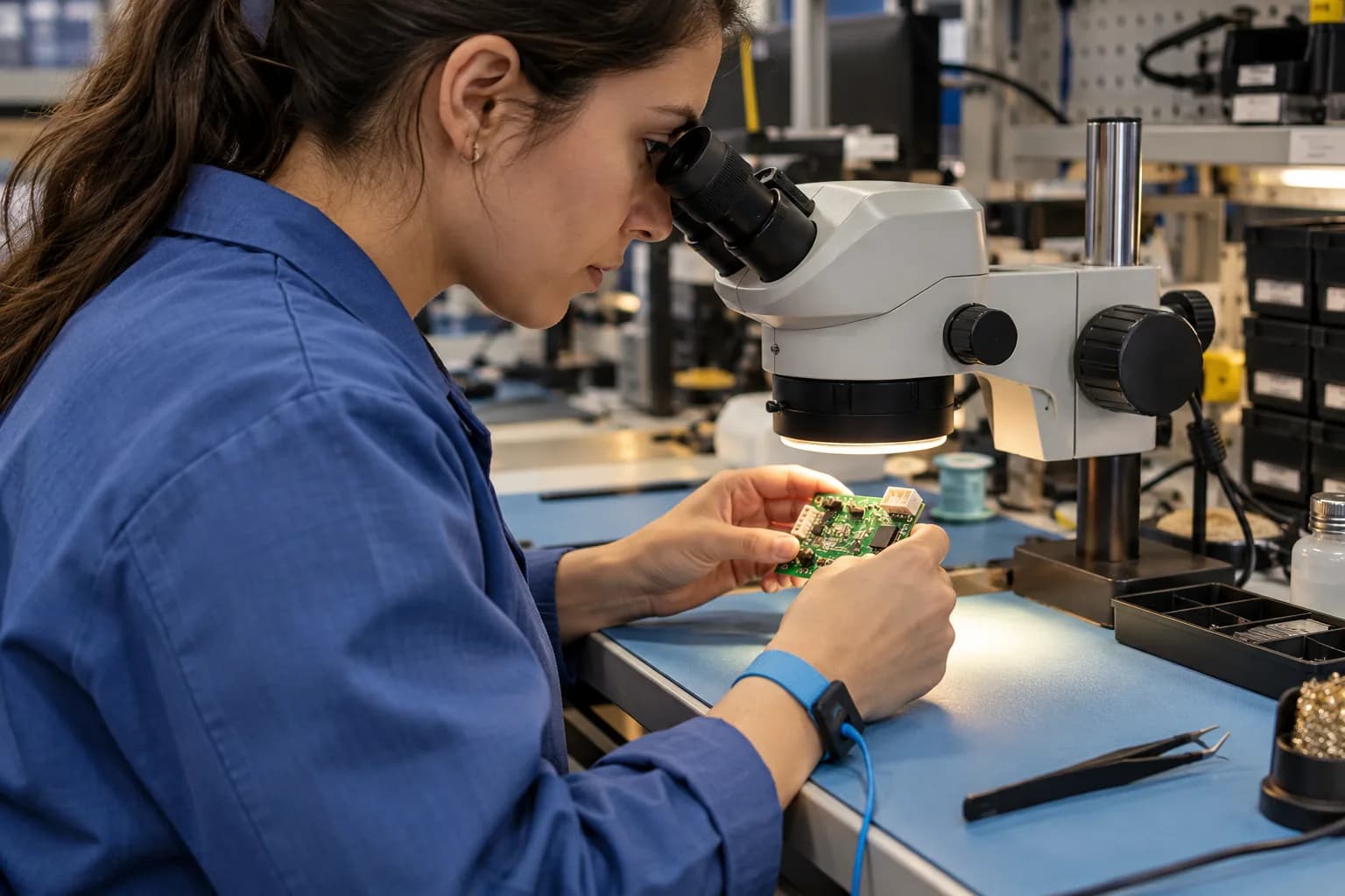
Where should PCB development begin?
Electronics development begins by describing what the device must do and the conditions in which it must operate. Define inputs, outputs, power, communications, mechanical limits and servicing needs together. A working bench prototype and a maintainable field device represent different scopes. Attach a verification method to each important requirement so the team knows what evidence will be needed before the design is considered complete.
For a sensor board, consider connector access, cable routing, data recording and restart behavior alongside measurement performance. Keep an explicit list of unresolved decisions and their owners. This makes assumptions reviewable during development and helps prevent late discoveries such as a connector that cannot be reached once the board is installed in its intended enclosure.
How should schematics and components be selected?
Break the design into functions such as power, processing, interfaces and measurement. Evaluate availability, lifecycle, alternatives and assembly constraints as well as electrical characteristics. Compare datasheet conditions with the actual circuit conditions. A reference design can inform development, but does not establish that the resulting board has been verified for a different enclosure, power source or operating environment.
Review power sequencing, connector orientation, programming access and test points before layout is finalized. Include firmware engineers at this stage. A board that implements the circuit logic but cannot be programmed or investigated conveniently can still delay the project. Development interfaces and manufacturing access should be deliberate decisions rather than temporary additions that disappear during mechanical refinement.
Why does manufacturability matter during PCB layout?
PCB layout involves more than completing electrical connections. Account for fabrication limits on layers, holes and geometry, plus assembly needs for access and component spacing. Eurocircuits' published workflow is one example of checking fabrication and assembly data for manufacturability. Such checks help identify transfer-to-production problems; they do not prove that the electrical design performs its intended function.
How should a prototype board be verified?
Prepare a bring-up plan, functional checks and failure scenarios before the boards arrive. Verify power, communications, sensing, recording and firmware updates against project requirements. Associate results with board revision, component changes and software version. One board working once does not demonstrate repeatability. Separate design faults from assembly, firmware and test-fixture issues so the next revision addresses a known cause rather than a guess.
What changes when moving toward production?
Repeatable production needs approved fabrication data, component lists, assembly instructions and acceptance steps. Define programming, functional testing, serial identification and defect records. Review the effect of a substituted component before updating the released manufacturing package. Required environmental or regulatory evaluations belong in explicit work packages; successful laboratory prototyping does not by itself create a certified product or establish suitability for every operating condition.
How do local engineering and global components fit together?
Local engineering contribution can be described through requirements, circuit design, layout, firmware, manufacturing preparation, testing and system integration. Global component sourcing can be stated transparently alongside those contributions. As an independent software and hardware house, Gokbilge Tech can assess work across these stages. Begin a discussion with the device purpose, interfaces and verification expectations rather than only its desired board dimensions.
Technical references
Want to apply this approach to your system?
Discuss your technical requirements →